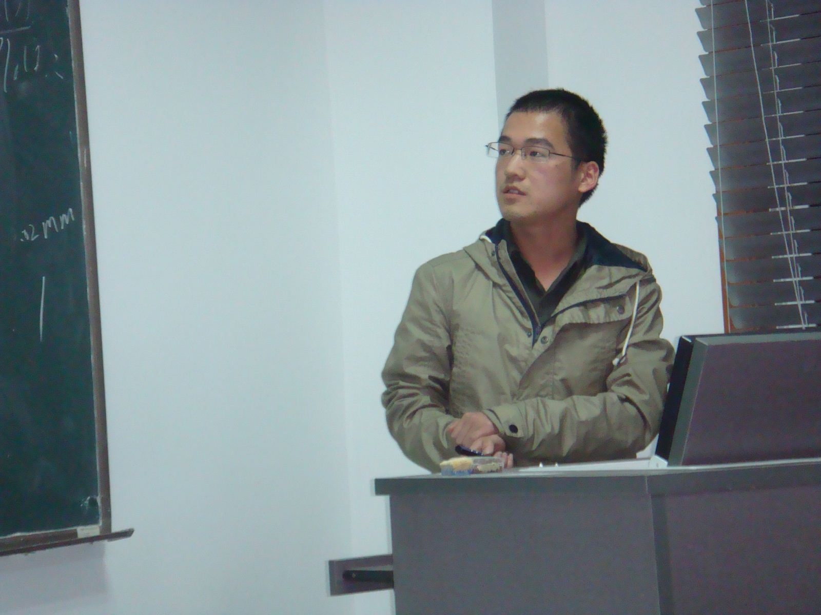
Research of the Structural Information of Laser Doped Black Silicon
Dong Xiao (董晓)
Supervisor: Professor Zhuang Jun
Department of Optical Science and Engineering

Abstract
The femtosecond-structured black silicon was first discovered by Mazur group in 1998 [1]. The microstructured black silicon consist of a core of undisturbed silicon covered with a highly disordered layer of silicon about several hundred nanometers thick including nanocrystallites, nanopores, and sulfur impurities [2]. The electron diffraction indicates that the core is crystalline and the surface layer is polycrystalline or microcrystalline [2]. Black silicon has significant optical properties that it can absorb the whole range of sun light (from 0.25µm to 2.5µm) [3]. The numbers of pulses, laser fluence, and background gas pressure also have great impact on the sub-band gap absorption [4, 5]. From the phenomenon we can draw a conclusion that the doped atoms may play a significant role in sub-band gap absorption of black silicon.
Mo and coworkers presented first-principles calculations for the behavior of sulfur point defects in crystalline and amorphous silicon structures [6]. The calculations are carried out with the total energy and molecular-dynamics computer code VASP, which employs a plane-wave basis. For the study of electronic states related to the presence of S dopants, they considered the substitutional position and four different interstitial positions [6]. Sánchez and coworkers studied intermediate band in silicon heavily coimplanted with chalcogens (S, Se, Te) [7]. They found that an occupied band corresponding to the deep levels of sulfur appears within the Si band gap when substituting one Si atom by S in the 216-atom cell [7]. The DOS diagram for SeSiSi215 and TeSiSi215 are almost identical to that of the S-substituted compound [7]. Smith and coworkers studied the phase transformations during femtosecond-laser doping of silicon by Raman spectroscopy technology [8]. They found that the intense light-matter interactions that occur during femtosecond-laser doping produce pressure waves sufficient to induce phase transformations in silicon, resulting in the formation of metastable polymorphic phases [8]. However, their studies of pressure-induced polymorphic phases in silicon during femtosecond laser irradiation are far from detailedness.
To determine the structures within a considerable bound of energy, upon which further investigations of their energetic, electronic, and optical properties are based, we studiously construct various geometric configurations by putting chalcogen atoms into different positions in silicon and then relax them to obtain the local energy minimum structures [9]. Sixteen typical geometric structures are listed from our expansive searching [9]. The results of our researches are a little different from that of Mazur group. We also investigated the Raman spectrum of micro-structured silicon in SF6, N2, and NF3, respectively, via femtosecond laser irradiation. We considered that the formed of polymorphic phases in micro-structured silicon may be relevant to the atoms that doped in the lattice of silicon. The black silicon that micro-structured in NF3 will be a good photovoltaic materials for its high crystalline. At last, I give the summary and future directions in my report.
References
[1] Tsing-Hua Her, Richard J. Finlay, Claudia Wu, Shrenik Deliwala, and Eric Mazur, Microstructuring of silicon with femtosecond laser pulses, Appl. Phys. Lett., Vol. 73, No 12, 21 september 1998.
[2] C. H. Crouch, J. E. Carey, J. M. Warrender, M. J. Aziz, and E. Mazur, F. Y. Ge´ nin, Comparison of structure and properties of femtosecond and nanosecond laser-structured silicon, Appl. Phys. Lett., Vol. 84, No. 11, 15 March 2004.
[3] Femtosecond Laser Ablation of Silicon: Nanoparticles, Doping and Photovoltaics, PhD thesis, Harvard University, 2007
[4] Michael A. Sheehy, Luke Winston, James E. Carey, Cynthia M. Friend,, and Eric Mazur, Role of the Background Gas in the Morphology and Optical Properties of Laser-Microstructured Silicon, Chem. Mater. 2005, 17, 3582-3586.
[5] C.H. Crouch, J.E. Carey, M. Shen, E. Mazur, F.Y. G´enin, Infrared absorption by sulfur-doped silicon formed by femtosecond laser irradiation, Appl. Phys. A 79, 1635–1641 (2004),
[6] Yina Mo, Martin Z. Bazant, Efthimios Kaxiras, Sulfur point defects in crystalline and amorphous silicon, PHYSICAL REVIEW B 70, 205210 (2004).
[7] K. Sánchez, I. Aguilera, P. Palacios, and P. Wahnón, Formation of a reliable intermediate band in Si heavily coimplanted with chalcogens (S, Se, Te) and group III elements (B, Al), PHYSICAL REVIEW B 82, 165201 2010.
[8] Matthew J. Smith,1 Yu-Ting Lin,2 Meng-Ju Sher,3 Mark T. Winkler,3 Eric Mazur, and Silvija Gradecˇak Pressure-induced phase transformations during femtosecond-laser doping of silicon, JOURNAL OF APPLIED PHYSICS 110, 053524 (2011).
[9] Hezhu Shao, Yuan Li, Jinhu Zhang, Bo-Yuan Ning, Wenxian Zhang, Xi-Jing Ning, Li Zhao and Jun Zhuang, Physical mechanisms for the unique optical propertiesof chalcogen-hyperdoped silicon, EPL, 99 (2012) 46005.
Thickness-dependence of optical constants for Ta2O5 ultrathin films
Dongxu Zhang
Supervisor: Yuxiang Zheng
Department of Optical Science and Engineering, Fudan University, 200433 Shanghai, China

Abstract
Owing to its large dielectric constant (high-k), high refractive index and good environment stability, tantalum pentoxide (Ta2O5) films have attracted great attention in both semiconductor sciences and optical sciences, and have found many applications such as antireflective layers, narrow-band interference filters, storage capacitors, gate dielectric, etc. Because of these wide field of applications, Ta2O5 films have been extensively studied both experimentally and theoretically. For device applications in microelectronics, ultrathin film with high dielectric constant can replace SiO2 as ultra-large-scale-integrated gate dielectric for its property equivalent to the one of a thinner SiO2 film1, 2. On the other hand, the dielectric constant of ultrathin film is depended on the thickness3. Several researches indicate that the dielectric constants and refractive indices of Ta2O5 ultrathin films deposited on silicon drop because of the SiO2 layer at the Ta2O5/Si-substrate interface4, 5. However, some other results show that the interfacial region is not pure SiO2, but a complex depth-dependent ternary oxide of Si-Tax-Oy6. Therefore, it is worth further studying on this topic of clarifying the optical properties of Ta2O5 ultrathin films.
In our work7, An effective method for determining the optical constants of Ta2O5 thin films deposited on crystal silicon (c-Si) using spectroscopic ellipsometry (SE) measurement with a two-film model (ambient-oxide-interlayer-substrate) was presented8, 9. The Ta2O5 thin films with thickness range of 1-400 nm have been prepared by electron beam evaporation (EBE) method. We find that the refractive indices of Ta2O5 ultrathin films less than 40 nm drop with the decreasing thickness, while the other ones are close to those of bulk Ta2O5. This phenomenon was due to the existence of an interfacial oxide region and the surface roughness of the film, which was confirmed by the measurement of atomic force microscopy (AFM). Optical properties of ultrathin film varied with the thickness are useful for the design and manufacture of nano-scaled thin film devices.
References
1 J. Y. Zhang and I. W. Boyd, Appl Phys Lett 77, 3574 (2000).
2 L. Q. Zhu, Q. Fang, G. He, M. Liu, and L. D. Zhang, Nanotechnology 16, 2865 (2005).
3 G. He, L. D. Zhang, M. Liu, J. P. Zhang, X. J. Wang, and C. M. Zhen, J Appl Phys 105, 014109 (2009).
4 C. Chaneliere, J. L. Autran, R. Devine, and B. Balland, Mat Sci Eng R 22, 269 (1998).
5 S. SEKI, T. UNAGAMI, O. KOGURE, and B. TSUJIYAMA, JOURNAL OF VACUUM SCIENCE & TECHNOLOGY A-VACUUM SURFACES AND FILMS 5, 1771 (1987).
6 G. B. Alers, D. J. Werder, Y. Chabal, H. C. Lu, E. P. Gusev, E. Garfunkel, T. Gustafsson, and R. S. Urdahl, Appl Phys Lett 73, 1517 (1998).
7 D. X. Zhang, Y. X. Zheng, Q. Y. Cai, W. Lin, K. N. Wu, P. H. Mao, R. J. Zhang, H. B. Zhao, and L. Y. Chen, Appl Phys A-Mater 108, 975 (2012).
8 L. Y. CHEN and D. W. LYNCH, Appl Optics 26, 5221 (1987).
9 L. Y. CHEN, X. W. FENG, Y. SU, H. Z. MA, and Y. H. QIAN, Appl Optics 33, 1299 (1994).
Thermal stability and magnetization reversal of antiferromagnetically coupled magnetic media layers
Haigang Chu
Advisor: Bin Ma

Abstract:
Exchanged coupled composite (ECC) media consisting of both magnetically hard and soft regions within the same grain have been proposed for 1Tb/in2 perpendicular magnetic recording .ECC media are widely investigated because of their potential media applications in heat assisted magnetic recording (HAMR), microwave assisted magnetic recording (MAMR), and bit pattern recording (BPR).The criterion for a thermally stable grain is given by KuV/60KBT, where Ku is the anisotropy constant, V the grain volume, KB the Boltzmann constant, and T the temperature. However, the ultra-high Ku makes the media too difficult to write with conventional head. ECC media can reduce the switching field of composite media while maintaining the stability.Due to its ultra-high anisotropy and chemical stability, L10 FePt is usually chosen as the hard layer, multilayers with perpendicular anisotropy, such as Co/Pt and Co/Ni, have been used as the soft layer in order to prepare the perpendicular ECC media. The reversible switching of the magnetization of the soft layer exerts a torque to that of the hard layer through the exchange coupling between the two layers and thus reduces the switching field of the hard layer, and the hard layer maintains the thermal stability. Furthermore, in the longitudinal magnetic recording, antiferromagnetically coupled (AFC) structure can increase the anisotropy. We consider a novel ECC structure with AFC layer as the soft layer.
In this presentation, I will introduce the thermal stability and magnetization reversal of the ECC L10 FePt/[Co/Ni]n/Ru/[Co/Ni]m. The switching mechanism of the ECC media is analyzed. With the Ru thickness increasing, the coercivity of composite media shows an oscillatory behavior. Ferromagnetic exchange and antiferromagnetic exchange alternately appear by varying the Ru thickness.
Reference
[1]R. H. Victora and X. Shen, IEEE Trans .Magn.41, 537 (2005).
[2]J.P.W,W. K. Shen, and J. M. Bai, IEEE Trans. Magn. 413181 (2005).
[3] Eric E. Fullerton and D. T. Margulies, Appl. Phys. Lett. 77, 23 (2000).
[4] H. H. Guo, J. L. Liao and B. Ma, J. Appl. Phys.111, 103916 (2012).
[5] H. H. Guo, J. L. Liao and B. Ma, Appl. Phys. Lett. 100 , 142406 (2012).

 复旦主页
复旦主页 实验室安全
实验室安全 复旦邮箱
复旦邮箱 办事大厅
办事大厅

